This is an old revision of the document!
Table of Contents
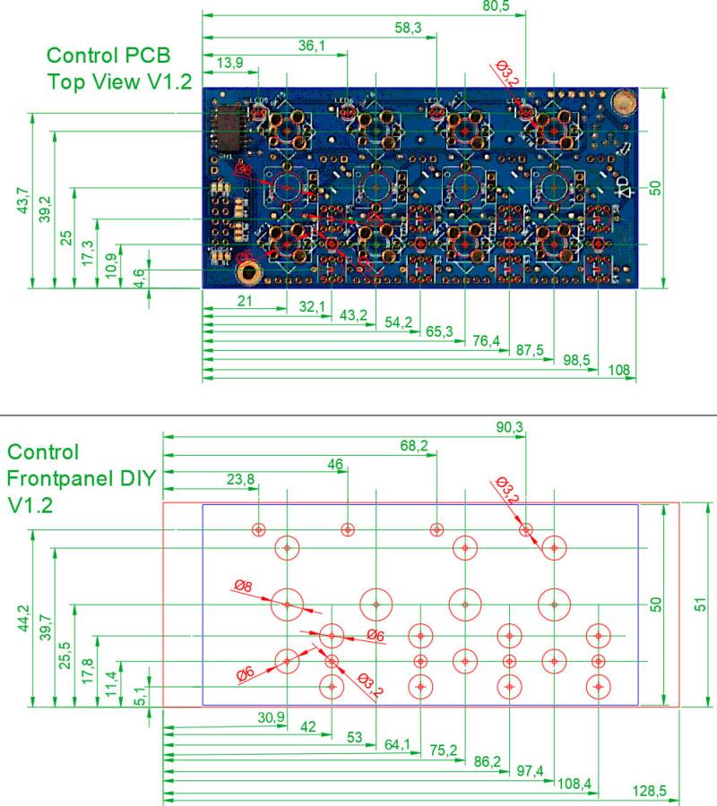
Control Panel AIN_4 & AOUT_4 v1.2
AIN4 - AOUT4 v1.2 TOP
BOM:
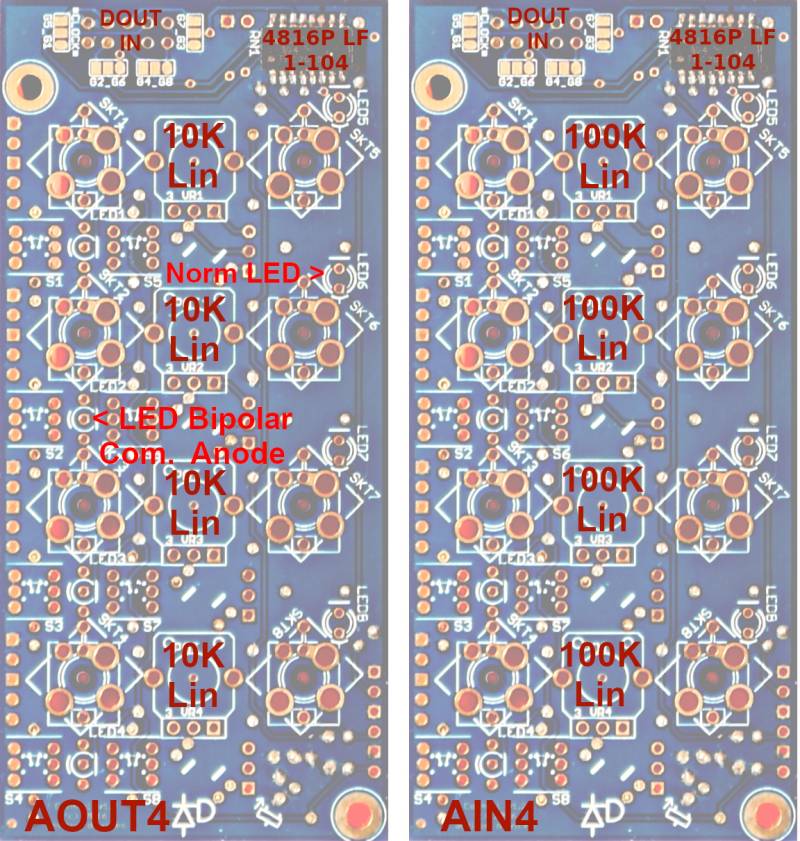
8x Switch better take mouser ones...
LED5-8: Normal LEDs
LED1-4: Bipolar LED comman Anode
VR1-4 AOUT4: 10K Lin
VR1-4 AIN4: 100K Lin
SKT1-4: 3,5 mono Jack
JP21: Optional Clock Input from SKT5 (then don't set G1_G5 on the backside)
J1: Routes gate outputs from a standard DOUT pinheader to SKT 5-8 according to solder jumper pairs Gxx
AIN_4 v1.2 BACK
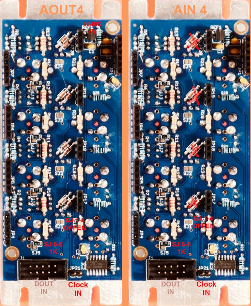
BOM:
RN1: 100k iso 652-4816P-1LF-100K
SJ 1-4: let them unsoldered
SJ 5-8: solder a 1K 0603 SMD Resistor from the Round PAD to GROUND- to avoid Floating
Diodes: 1N4148 > only Stuff in AOUT4 Usecases
IC2: 74LV14H (SOIC14)
C2: 100nF Kerko
The Rest: cant remember…Resistors and Caps…
about G5_G1, G2_G6, G4_G8, G7_G3:
J1 you connect to a DOUTx4 output, which deliver 8 DOUTs on 1 shroudet header
But we only use 4 DOUTs on the Controlboards… with this jumpers you decide which one!
IF you use a CLOCK coming from J21, then dont set G1_G5!

