This is an old revision of the document!
Table of Contents
SEQv4+ Jog module
A BLM using 18 illuminated MEC switches placed around an encoder (datawheel). Two spare DIN pins can accommodate a footswitch and a modular gate.
Schematic
The circuit is a BLM, but only four DIN columns are used. The other four DIN pins scan an encoder and two inputs intended as footswitch/gate. Standard SRIO in on J89 and chained out on J89A.
The BLM is as follows:
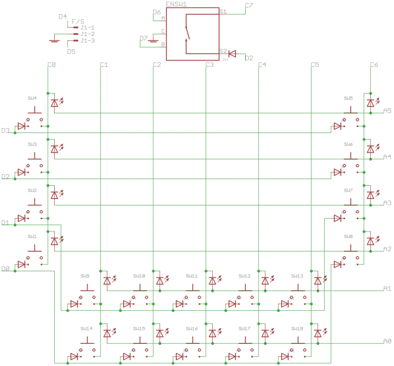
Note the encoder connected to pins D7 and D6, and header J1 connected directly to D5 and D4. All of the cathode rows are used, even C7 just for the encoder push switch.
Only six DOUT anode columns are used. These are current limited by resistors R1-6.
BOM v1.0 placeholder
| Type | Qty | Value | Package | Parts | Mouser | Reichelt | Conrad | Other | Notes |
|---|---|---|---|---|---|---|---|---|---|
| Resistors | |||||||||
| 6 | 100-220R 5% | THT | R1-6 | ||||||
| Resistor network | |||||||||
| 1 | 10k | SOM16 | RN1 | 4816P-T02-103LF | |||||
| Capacitors | |||||||||
| 3 | 100n | 1206 | C1-3 | ||||||
| Diodes | |||||||||
| 19 | 1N4148 | THT | |||||||
| LEDs | |||||||||
| 18 | various | 3mm | put LEDs in the switches first! | ||||||
| ICs | |||||||||
| 1 | 74HC165 | SOIC16 | IC2 | 595-SN74HC165DR | |||||
| 2 | 74HC595 | SOIC16 | IC1, IC3 | ||||||
| Encoder | |||||||||
| 1 | STEC12 | STEC12E08 | |||||||
| Switches | |||||||||
| 18 | MEC/APEM | 3FTH9 | SW1-18 | 642-3FTH9 | TASTER 3FTH9 | 705276 - 62 | |||
| Headers | |||||||||
| 1 | 1*3 | male | |||||||
| 2 | 2*5 | male | |||||||
| Hardware | |||||||||
| 6 | M3 spacer | TBD | |||||||
| 1 | datawheel | DK-38? | |||||||
| 18 | switchcaps | 22.5mm | 642-1S11-22.5 | 1S11-22.5 | |||||
Versions
v1.0: first release.
Assembly placeholder
Solder the SMT parts first. Ensure the TVS diode is aligned with the larger pin on the larger pad and that the wide edge of the body fits between the silkscreen indicators:

Note this is the board viewed from the bottom; the larger pin is on the bottom-left.
To have a through-hole USB A socket, the pins are quite close together. Be careful to avoid bridges when soldering and test with a multimeter to ensure no adjacent pins are connected afterwards!
It goes without saying, but ensure none of the metal parts are touching (e.g. the outside of the USB sockets with J7, the 1N4148 diode with the mounting brackets etc.).
License
Currently the design is © 2017 antilog devices with all rights reserved; all documentation is CC BY-NC-SA 3.0.