This is an old revision of the document!
Table of Contents
wCoreF4 PCB
This is the carrier board for the Waveshare Core407v. It performs breakout functions of all of the standard ports as per the design based on the STM32 Discovery.
Schematic
The circuit is mostly identical to what was drawn previously. The following parts are different:
USB entry (J1)
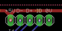
This header supplies +5V, 0V, USB data and the ID state. Normally it will be connected to the USB module by a short cable.
Extended port (J16E)
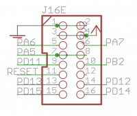
The original J16 functionality is preserved, but extra pins are available on an IDC16 header. These include the Reset signal and pins normally controlling LEDs. This header is normally connected to the RES-SD module.
User button (JPA0)
This jumper replaces the “bootloader” functionality of the Discovery board's blue button. It could be wired to an external panel control if needed.
BOM v1.0
| Type | Qty | Value | Package | Parts | Mouser | Reichelt | Conrad | Other | Notes |
|---|---|---|---|---|---|---|---|---|---|
| Resistors | |||||||||
| 2 | 220R 5% | THT | R7A, R8A | ||||||
| 2 | 220R 5% | 1206 | R7B, R8B | ||||||
| 1 | 330R 5% | THT | R102 | ||||||
| 4 | 1k 5% | 1206 | R7B1-4 | ||||||
| 2 | 1k 5% | THT | R11, R13 | ||||||
| 1 | 10k 5% | THT | R12 | ||||||
| 1 | 220k 5% | THT | R101 | ||||||
| Pots | |||||||||
| 2 | 10k | 6*5mm vert | P1, P2 | ||||||
| Capacitors | |||||||||
| 3 | 100n | 1206 | C1A, C1B, C2 | ||||||
| Diodes | |||||||||
| 1 | 1N4148 | THT | as marked | ||||||
| Transistors | |||||||||
| 1 | BC337 | TO-92 | T1 | ||||||
| ICs | |||||||||
| 2 | 74HCT125 | SOIC | IC1A, IC1B | 595-SN74HCT125DR | Ensure HCT | ||||
| 1 | 74HC595 | SOIC | IC2 | ||||||
| Headers | |||||||||
| 2 | 1*2 | male | |||||||
| 1 | 1*3 | male | |||||||
| 1 | 1*5 | male | J1 | or wire directly | |||||
| 9 | 2*5 | male | |||||||
| 3 | 2*8 | male | |||||||
| 2 | 2*25 | female | |||||||
| Hardware | |||||||||
| 4 | M3 spacer | 8mm(?) | |||||||
| MCU breakout | |||||||||
| 1 | Waveshare Core 407v | ||||||||
Versions
v1.0: first release.
Assembly
The following build order is suggested:
- R7B1-4 (1k) and located near J15_S on the top side
- R7B and R8B (220R) on the bottom side
- C1A, C1B and C2 on the bottom side
- IC1A, IC1B and IC2 on the bottom side
- Top-side THT components
- Bottom-side THT components
- Bottom-side JPA0 header
- Bottom-side 2*25 pin female headers
- Top-side male headers, except for J1
- Solder J1 in conjunction with the USB module
- Mounting brackets if needed
Connecting the Core407v breakout
- Checking the Waveshare board, you will see that there is a real-time clock crystal and associated caps connected across PC14 and PC15. I think it's best to remove these parts so they don't interfere with normal operation. Clip the leads of the crystal and desolder the part if you like. The caps should come off quite easily with a soldering iron tip heating both pads.
- Looking at the top side of the PCB (with all headers etc.) and J1 at the “northern” edge, the Core 407v board plugs in on the bottom side with the JTAG header towards the right
- Remove the OTG jumpers “FLG,” “VBUS” and “PWR OUT.” USB won't work properly with these closed.
- I believe that the correct state of the BOOT CONFIG switch should be set to “SYSTEM”
- There's another switch to select the +5V power. It should be set to “USB” when flashing the board using the USB mini connector as a power source, but for our purposes set it to “PWR 5V”.
License
Currently the design is © 2016 antilog devices with all rights reserved; all documentation is CC BY-NC-SA 3.0.