Table of Contents
CS1
A button matrix with space to mount encoders, graphical OLED and character displays.
Schematic
Switch matrix, including (max) three encoder switches:
| Switch | Row | Column |
|---|---|---|
| S1 | 2 | A |
| S2 | 1 | B |
| S3 | 1 | C |
| S4 | 3 | D |
| S5 | 2 | D |
| S6 | 1 | D |
| S7 | 1 | E |
| S8 | 1 | F |
| S9 | 2 | G |
| S10 | 2 | H |
| S11 | 3 | A |
| S12 | 2 | B |
| S13 | 2 | C |
| S14 | 4 | D |
| S15 | 4 | E |
| S16 | 3 | E |
| S17 | 2 | E |
| S18 | 3 | G |
| S19 | 3 | H |
| S20 | 4 | A |
| S21 | 3 | B |
| S22 | 4 | B |
| S23 | 3 | C |
| S24 | 4 | C |
| S25 | 4 | F |
| S26 | 3 | F |
| S27 | 2 | F |
| S28 | 4 | G |
| S29 | 4 | H |
| ENSW1 | 1 | A |
| ENSW2/3 | 1 | G |
| ENSW4 | 1 | H |
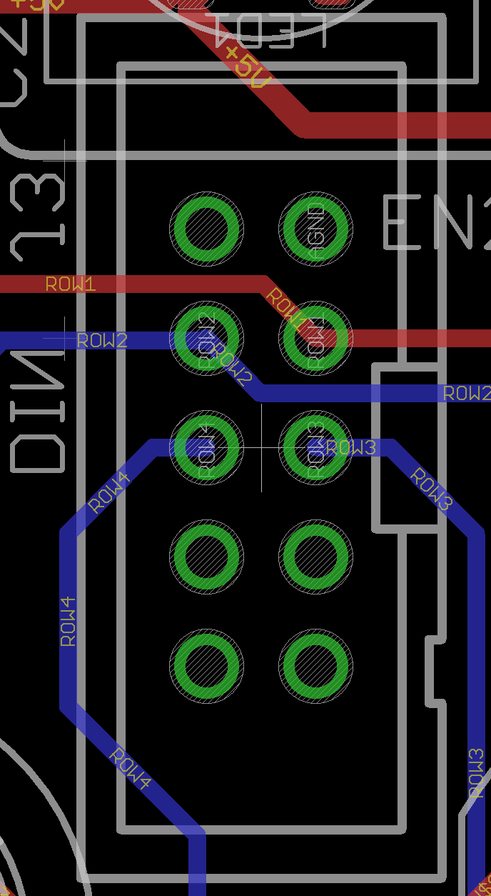
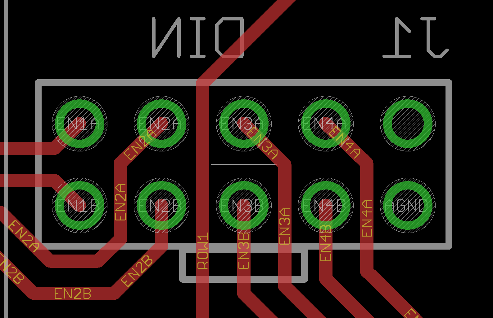
Note that these headers are viewed from the front, so are “mirrored.” Pin 1 is AGND (0V).
J2: DOUT columns
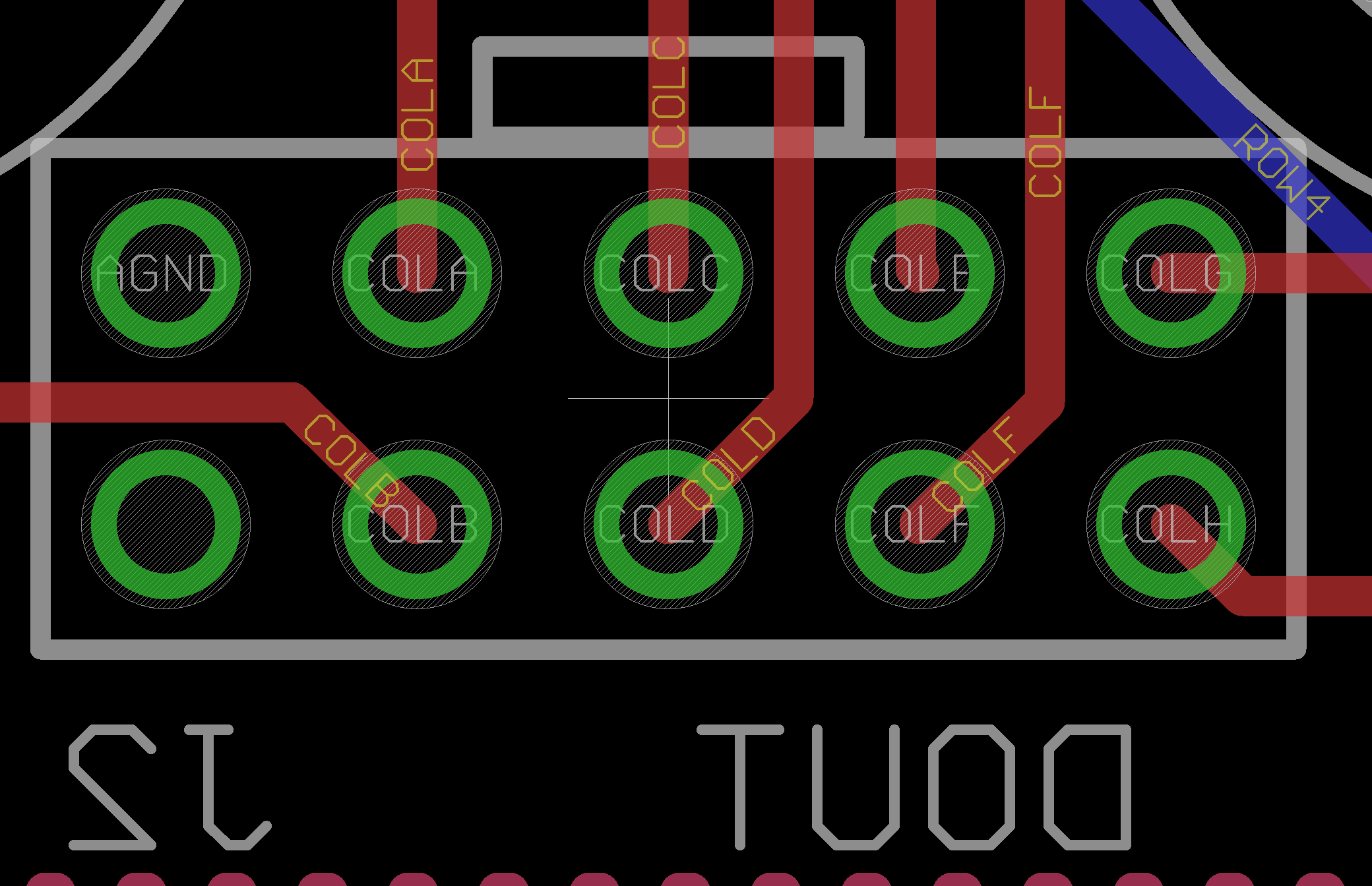
J3: DIN rows
J1: encoders
J10B: GPIO for typical SSD1306 OLEDs
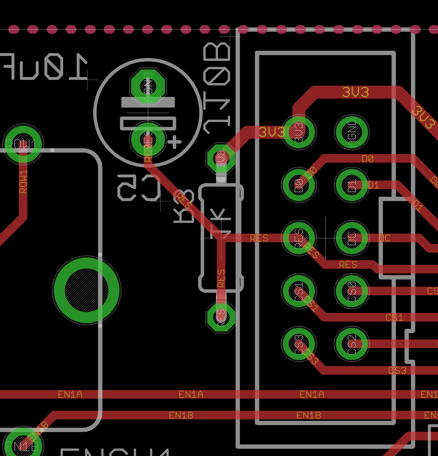
Note the resistor/cap reset circuit.
J4 carries the WS2812B serial signal. R1 should be 220-470R for only the first module in the chain, thereafter a wire link. J5 is the serial chain output. R2 and C4 could terminate the serial signal but shouldn't be required.
J6 supplies +5V power through a 5817 diode. This is required; there is no power connection to J4.
BOM v1.0
| Type | Part | Value |
|---|---|---|
| Caps | C1 | 10-100uF |
| C2 | 100n | |
| C3 | 100n | |
| C4 | DNF | |
| C5 | 10uF | |
| Diodes | D1 | 1N4148DO35-7 |
| D2 | 1N4148DO35-7 | |
| D3 | 1N4148DO35-7 | |
| D4 | 1N4148DO35-7 | |
| D5 | 1N4148DO35-7 | |
| D6 | 1N4148DO35-7 | |
| D7 | 1N4148DO35-7 | |
| D8 | 1N4148DO35-7 | |
| D9 | 1N4148DO35-7 | |
| D10 | 1N4148DO35-7 | |
| D11 | 1N4148DO35-7 | |
| D12 | 1N4148DO35-7 | |
| D13 | 1N4148DO35-7 | |
| D14 | 1N4148DO35-7 | |
| D15 | 1N4148DO35-7 | |
| D16 | 1N4148DO35-7 | |
| D17 | 1N4148DO35-7 | |
| D18 | 1N4148DO35-7 | |
| D19 | 1N4148DO35-7 | |
| D20 | 1N4148DO35-7 | |
| D21 | 1N4148DO35-7 | |
| D22 | 1N4148DO35-7 | |
| D23 | 1N4148DO35-7 | |
| D24 | 1N4148DO35-7 | |
| D25 | 1N4148DO35-7 | |
| D26 | 1N4148DO35-7 | |
| D27 | 1N4148DO35-7 | |
| D28 | 1N4148DO35-7 | |
| D29 | 1N4148DO35-7 | |
| D30 | 1N4148DO35-7 | |
| D31 | 1N4148DO35-7 | |
| D32 | 1N4148DO35-7 | |
| D111 | 1N5817 | |
| OLEDs | DISP1 | SSD1306 SPI4 |
| DISP2 | SSD1306 SPI4 | |
| DISP3 | SSD1306 SPI4 | |
| DISP4 | SSD1306 SPI4 | |
| Encoders | EN2 | ENCODER_NO_SWITCHSW |
| EN3 | ENCODER_NO_SWITCHSW | |
| ENSW1 | ENCODER+SWITCHSW | |
| ENSW2 | ENCODER+SWITCHSW | |
| ENSW3 | ENCODER+SWITCHSW | |
| ENSW4 | ENCODER+SWITCHSW | |
| Headers | J1 | DIN |
| J2 | DOUT | |
| J3 | DIN | |
| J4 | WS2812 | |
| J5 | WS2812 | |
| J6 | +5v | |
| J10B | PINHD-2X54WALL | |
| LEDs | LED1 | WS2812B |
| LED2 | WS2812B | |
| Resistors | R1 | 220-470R or link |
| R2 | DNF | |
| R3 | 1k | |
| Switches | S1 | DT6 |
| S2 | DT6 | |
| S3 | DT6 | |
| S4 | DT6 | |
| S5 | DT6 | |
| S6 | DT6 | |
| S7 | DT6 | |
| S8 | DT6 | |
| S9 | DT6 | |
| S10 | DT6 | |
| S11 | DT6 | |
| S12 | DT6 | |
| S13 | DT6 | |
| S14 | DT6 | |
| S15 | DT6 | |
| S16 | DT6 | |
| S17 | DT6 | |
| S18 | DT6 | |
| S19 | DT6 | |
| S20 | DT6 | |
| S21 | DT6 | |
| S22 | DT6 | |
| S23 | DT6 | |
| S24 | DT6 | |
| S25 | DT6 | |
| S26 | DT6 | |
| S27 | DT6 | |
| S28 | DT6 | |
| S29 | DT6 |
Versions
v1.0: first release.
Assembly
Decide on the layout. Only four encoders are supported. ENSW1 and ENSW4 are always available; EN2/ENSW2 and EN3/ENSW3 share pins. The switch for ENSW2/ENSW3 is also shared. This way one can choose whether to have switched encoders or encoders illuminated with WS2812B LEDs.
If illuminated encoders are desired, install these and the associated capacitors first.
Next diodes and resistors/links. Align the diode band with the silkscreen legend. Next the two electrolytic caps.
OLEDs could be socketed using a right-angle pin header. This means a corresponding female header would need to replace the standard 7-pin one common to these displays.
Headers, switches and encoders come last. Note the flat part of the switch, which must align with the DT6 switch body. Illuminated encoders should be raised up around 2mm to fit over the LED and still turn freely.
Interconnection to Core
Headers are mentioned above. DIN/DOUT connect to DINX4/DOUTX4 or a DIOMATRIX. J10B to J10B
Dimensions

License
Currently the design is © 2018 antilog devices with all rights reserved; all documentation is CC BY-NC-SA 3.0.