This is an old revision of the document!
Table of Contents
Display driver module
32 SPI-driven displays
Schematic
The concept is to buffer the time-critical clock signal. A wire connected directly to the MCU is loaded by the long distance (resistance in the connectors and wires) and could be susceptible to noise. Using a 541 buffer and shunt resistors controls this impedance. The serial data and data/command (DC) signals are also buffered to avoid time propagation errors.
The second purpose is to use a chain of shift registers to provide chip select (CS) signals. It is functionally equivalent to a DOUT module, but the header is directly compatible with GPIO on the Core.
BOM v1.0
| Type | Part | Value | Device |
|---|---|---|---|
| Caps | C1 | 100n | C025-025×050 |
| C2 | 100n | C025-025×050 | |
| C3 | 100n | C025-025×050 | |
| C4 | 100n | C025-025×050 | |
| C5 | 100n | C025-025×050 | |
| C6 | 100n | C025-025×050 | |
| C7 | 100n | C025-025×050 | |
| ICs | IC1 | 74HC541N | 74HC541N |
| IC2 | 74HC541N | 74HC541N | |
| IC3 | 74HC541N | 74HC541N | |
| IC4 | 74HC595N | 74HC595N | |
| IC5 | 74HC595N | 74HC595N | |
| IC6 | 74HC595N | 74HC595N | |
| IC7 | 74HC595N | 74HC595N | |
| Headers | J1 | PINHD-2X54WALL | PAK100/2500-10 |
| J2 | PINHD-2X54WALL | PAK100/2500-10 | |
| J3 | PINHD-2X54WALL | PAK100/2500-10 | |
| J4 | PINHD-2X54WALL | PAK100/2500-10 | |
| J5 | PINHD-2X54WALL | PAK100/2500-10 | |
| J6 | PINHD-2X54WALL | PAK100/2500-10 | |
| J7 | PINHD-2X54WALL | PAK100/2500-10 | |
| J8 | PINHD-2X54WALL | PAK100/2500-10 | |
| J9 | +5V | 22-23-2031 | |
| J10B | PINHD-2X54WALL | PAK100/2500-10 | |
| J10B1 | PINHD-2X54WALL | PAK100/2500-10 | |
| J15A | PINHD-2X8THTTHT | PAK100/2500-16 | |
| J15A1 | PINHD-2X8THTTHT | PAK100/2500-16 | |
| Resistors | R1 | ~220R | 0207/10 |
| R2 | ~220R | 0207/10 | |
| R3 | ~220R | 0207/10 | |
| R4 | ~220R | 0207/10 | |
| R5 | ~220R | 0207/10 | |
| R6 | ~220R | 0207/10 | |
| R7 | ~220R | 0207/10 | |
| R8 | ~220R | 0207/10 | |
| R9 | ~220R | 0207/10 | |
| R10 | ~220R | 0207/10 | |
| R11 | ~220R | 0207/10 | |
| R12 | ~220R | 0207/10 | |
| R13 | ~220R | 0207/10 | |
| R14 | ~220R | 0207/10 | |
| R15 | ~220R | 0207/10 | |
| R16 | ~220R | 0207/10 | |
| R17 | ~220R | 0207/10 | |
| R18 | ~220R | 0207/10 | |
| R19 | ~220R | 0207/10 | |
| R20 | ~220R | 0207/10 | |
| R21 | ~220R | 0207/10 | |
| R22 | ~220R | 0207/10 | |
| R23 | ~220R | 0207/10 | |
| R24 | ~220R | 0207/10 | |
| R25 | ~1k | 0207/10 | |
| R26 | ~1k | 0207/10 | |
| R27 | ~1k | 0207/10 | |
| R28 | ~1k | 0207/10 | |
| R29 | ~1k | 0207/10 | |
| R30 | ~1k | 0207/10 | |
| R31 | ~1k | 0207/10 | |
| R32 | ~1k | 0207/10 | |
| R33 | ~1k | 0207/10 | |
| R34 | ~1k | 0207/10 | |
| R35 | ~1k | 0207/10 | |
| R36 | ~1k | 0207/10 | |
| R37 | ~1k | 0207/10 | |
| R38 | ~1k | 0207/10 | |
| R39 | ~1k | 0207/10 | |
| R40 | ~1k | 0207/10 | |
| R41 | ~1k | 0207/10 | |
| R42 | ~1k | 0207/10 | |
| R43 | ~1k | 0207/10 | |
| R44 | ~1k | 0207/10 | |
| R45 | ~1k | 0207/10 | |
| R46 | ~1k | 0207/10 | |
| R47 | ~1k | 0207/10 | |
| R48 | ~1k | 0207/10 | |
| R49 | ~1k | 0207/10 | |
| R50 | ~1k | 0207/10 | |
| R51 | ~1k | 0207/10 | |
| R52 | ~1k | 0207/10 | |
| R53 | ~1k | 0207/10 | |
| R54 | ~1k | 0207/10 | |
| R55 | ~1k | 0207/10 | |
| R56 | ~1k | 0207/10 |
Versions
v1.0: first release. Erratum: there is a significant error in that J15 is mirrored. The simplest way to get it working is to swap pairs of the ribbon wires as shown:
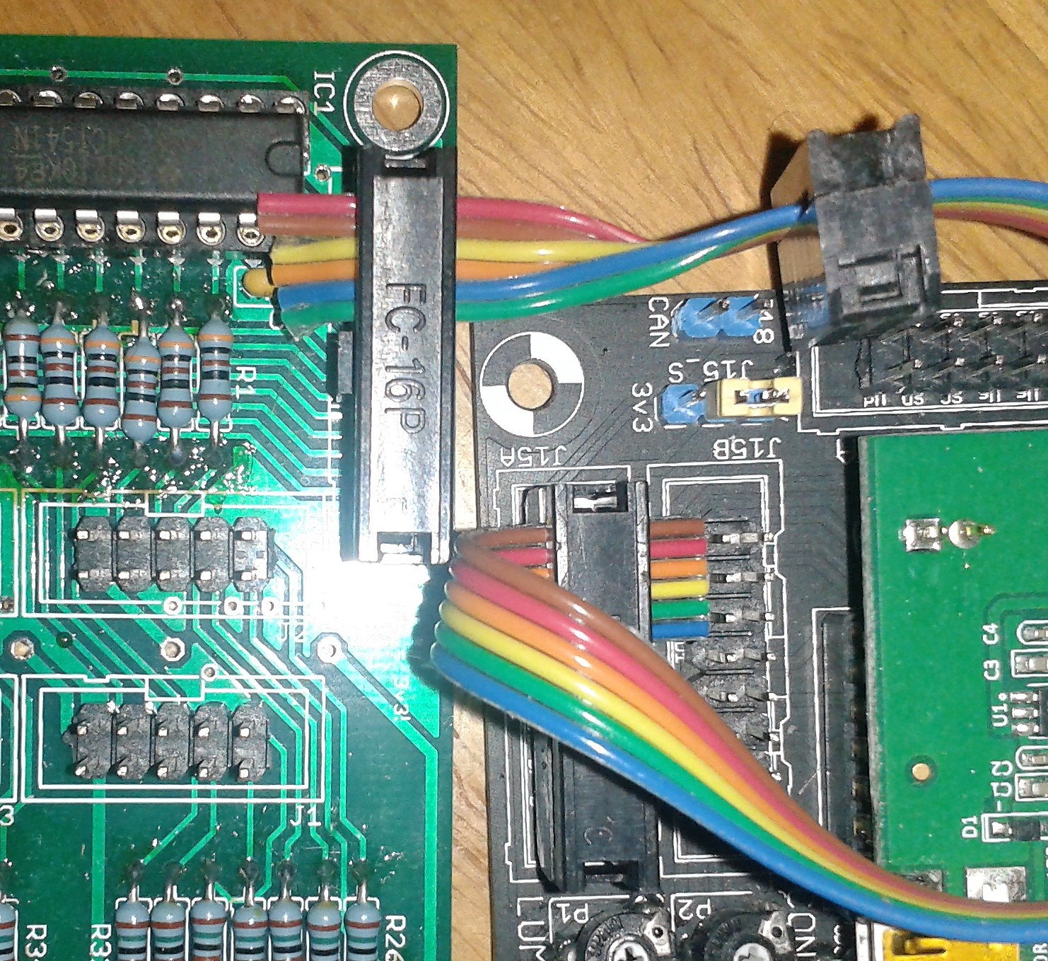
Here the header notches are aligned with the silkscreen. Only the first six are required.
Assembly
The 1206 caps and SMT parts should be soldered first. Note the orientation of ICs! In general they will have pin 1/16 nearest the decoupling cap. Pin 1 for RNs is marked with a circle, important as these chips are also polarised. Some headers are marked as “socket this side.” To use the module normally, install the headers on the rear side.
Note the instructions for DOUT1/2. You either need ICs 11/12 and resistors vertically mounted or spanning the outermost pads in place of IC11/12.
Interconnection to Core
J10B connects to J10B. J15A to J15A. Note the mirrored connection on v1.0
J15A1/J10B1 chain another Display Driver. Note that the J15 connection should not be mirrored for subsequent boards.
Dimensions
The PCB is 100*100mm with 3.6mm diameter holes centred 3.5mm from the edges.
License
Currently the design is © 2018 antilog devices with all rights reserved; all documentation is CC BY-NC-SA 3.0.