Table of Contents
SEQ v4L mk II
An updated SEQ V4L that only needs one ribbon connector to an LPC-17 or STM32F4 Core.

Image credit: TK.
Schematic
Matrix wiring
Wiring follows the same form as the original SEQ v4L. Each element is shown separately (please ignore the part designators):
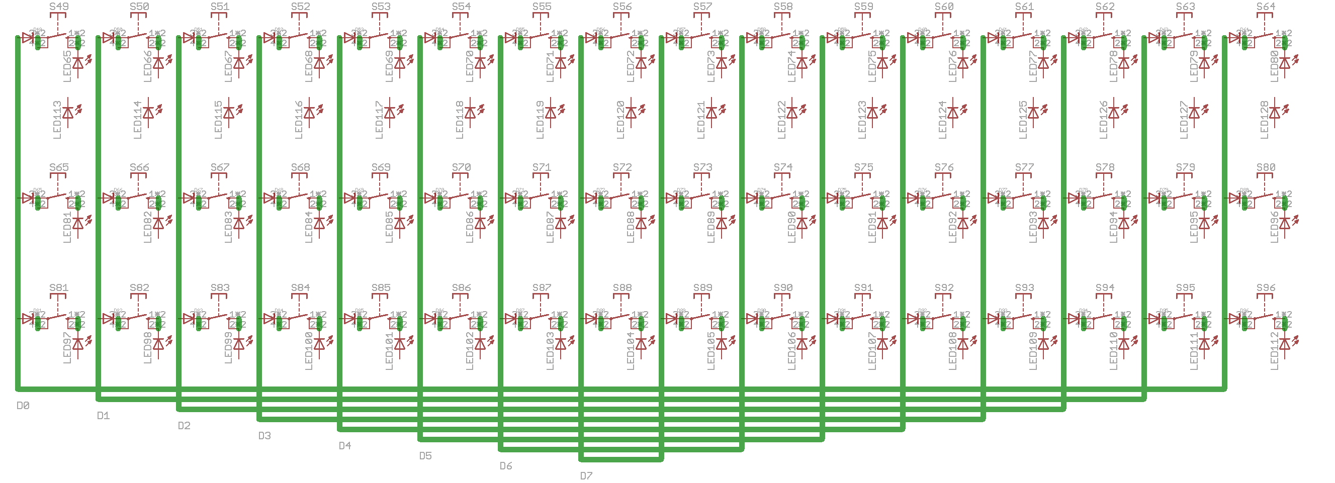
D0-D7 are used to scan switch input columns
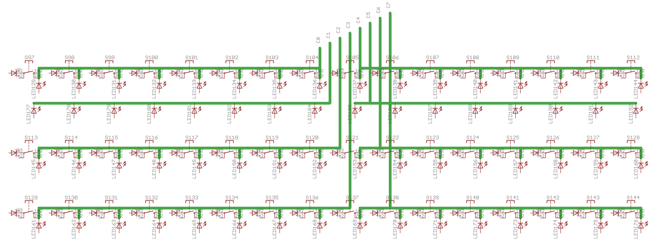
C0-C7 are selection pulses on 8 “rows”
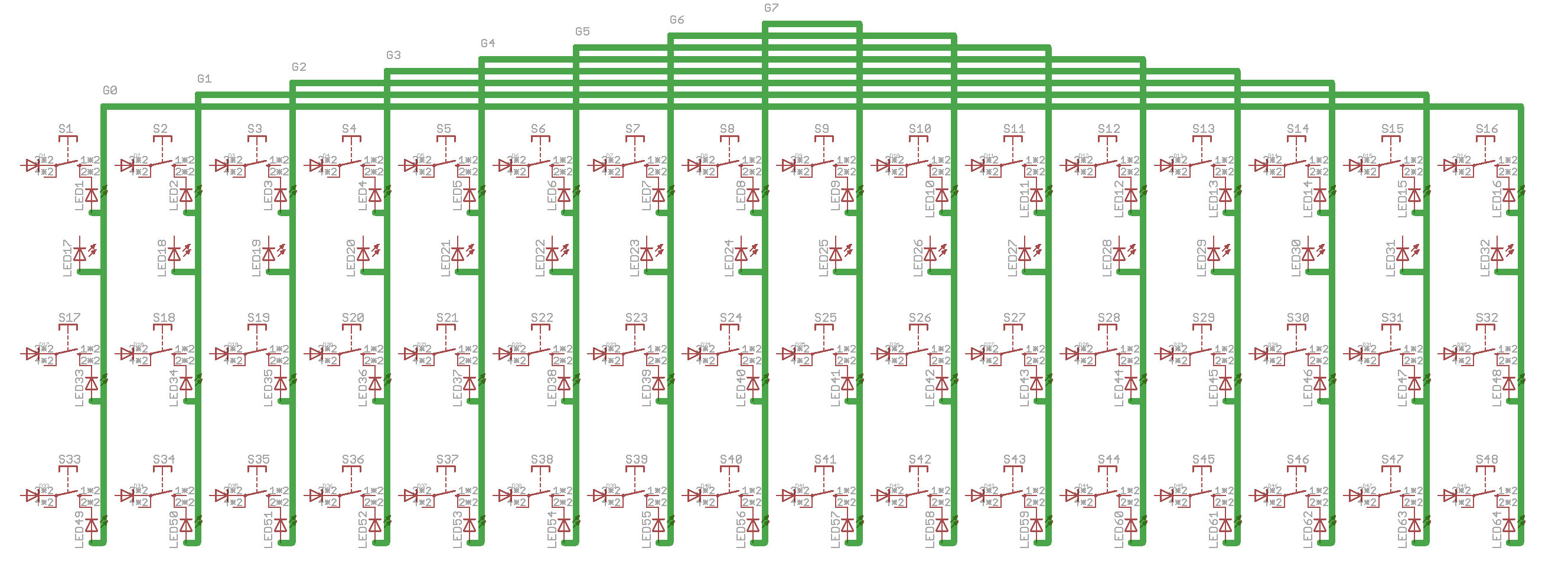
G0-G7 control LED columns
| IC | Pin | Connection | Notes |
|---|---|---|---|
| IC1 | 11 | D0 | digital inputs with pullup to +5V |
| 12 | D1 | ||
| 13 | D2 | ||
| 14 | D3 | ||
| 3 | D4 | ||
| 4 | D5 | ||
| 5 | D6 | ||
| 6 | D7 | ||
| IC2 | 15 | C7 | via LINK (C7), else directly connected |
| 1 | C6 | ||
| 2 | C5 | ||
| 3 | C4 | ||
| 4 | C3 | ||
| 5 | C2 | ||
| 6 | C1 | ||
| 7 | C0 | ||
| IC3 | 15 | G7 | via 100R resistors |
| 1 | G6 | ||
| 2 | G5 | ||
| 3 | G4 | ||
| 4 | G3 | ||
| 5 | G2 | ||
| 6 | G1 | ||
| 7 | G0 |
Circuit description
The circuit is merely a single colour 8*8 BLM (button LED matrix) arranged as a 16*4 with one row of switches left out. Normally a different colour LED will be used to indicate steps. A J8/9 connector carries the SRIO chain for 2* 74HC595 and 1* 74HC165 chips (with coupling capacitors). No current sink transistors are used. The remaining components are diodes on every switch to avoid false triggering, pull up resistors for the DIN inputs and current limiting resistors for LEDs.
BOM v1.1
| Type | Qty | Value | Package | Parts | Notes |
|---|---|---|---|---|---|
| resistors | |||||
| 9 | 10k | 0204/7 | pull ups go on the left side of the board, plus one extra near the 74HC165 | ||
| 8 | 100R | 0204/7 | right side of the board, one at the bottom | some control over LED brightness is possible, but current is limited by 74HC595s | |
| 1 | LINK | 0204/7 | one wire link is required, use a clipped resistor lead | ||
| capacitors | |||||
| 3 | 100n | 1206 | rear of board near ICs | ||
| ICs | |||||
| 1 | 74HC165 | SOIC16 | IC1 | to the right of J8/9 viewed from the rear | |
| 2 | 74HC595 | SOIC16 | IC2, IC3 | to the left of J8/9 viewed from the rear | |
| LEDs | |||||
| 16 | (red) | 3mm | |||
| 48 | (green) | 3mm | |||
| diodes | |||||
| 48 | 1N4148 | next to each switch | |||
| switches | |||||
| 48 | see note below | ||||
| headers | |||||
| 2 | 2*5 (shrouded) | J8/9, J8/9A; rear of PCB | note the input header J8/9 is located near the centre of the board between IC1 and IC2 | ||
Note for switches
The board supports two different type of switch: el cheapo 6mm types and nicer ITT D6. The brand name is also known as C&K e.g. Mouser.
For D6 switches many different colours and even square shapes are possible. Ensure the flattened part of the circular base aligns with the silkscreen legend.
Versions
v1.1: first release. Errata: the bottom silkscreen names/values are missing. Please refer to the PCB image. In words, the two 74HC595 chips are next to each other, while the 74HC165 chip is on the right side of J8/9 when viewed from the rear.
PCBs
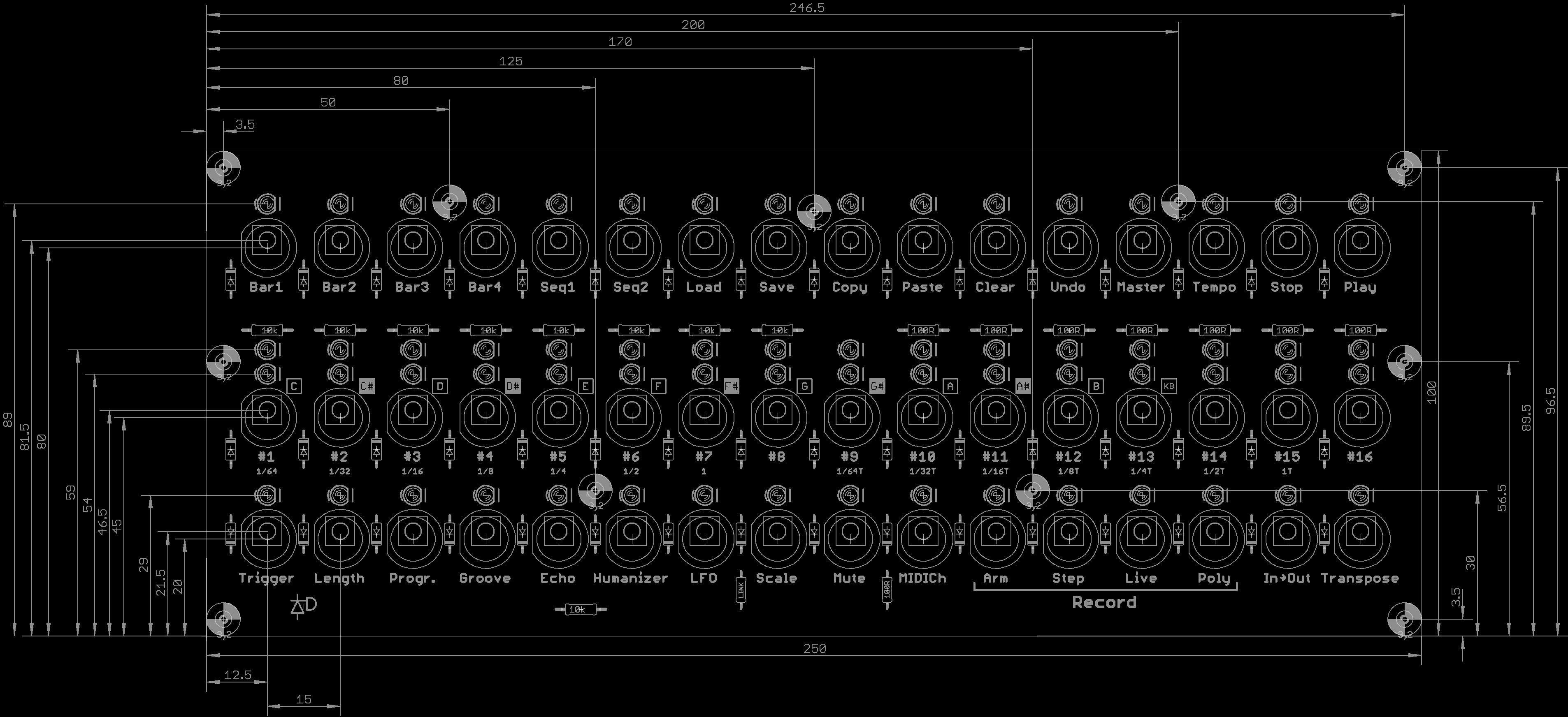
Front + dimensions (in mm) of switches, LEDs and mounting holes (M3)
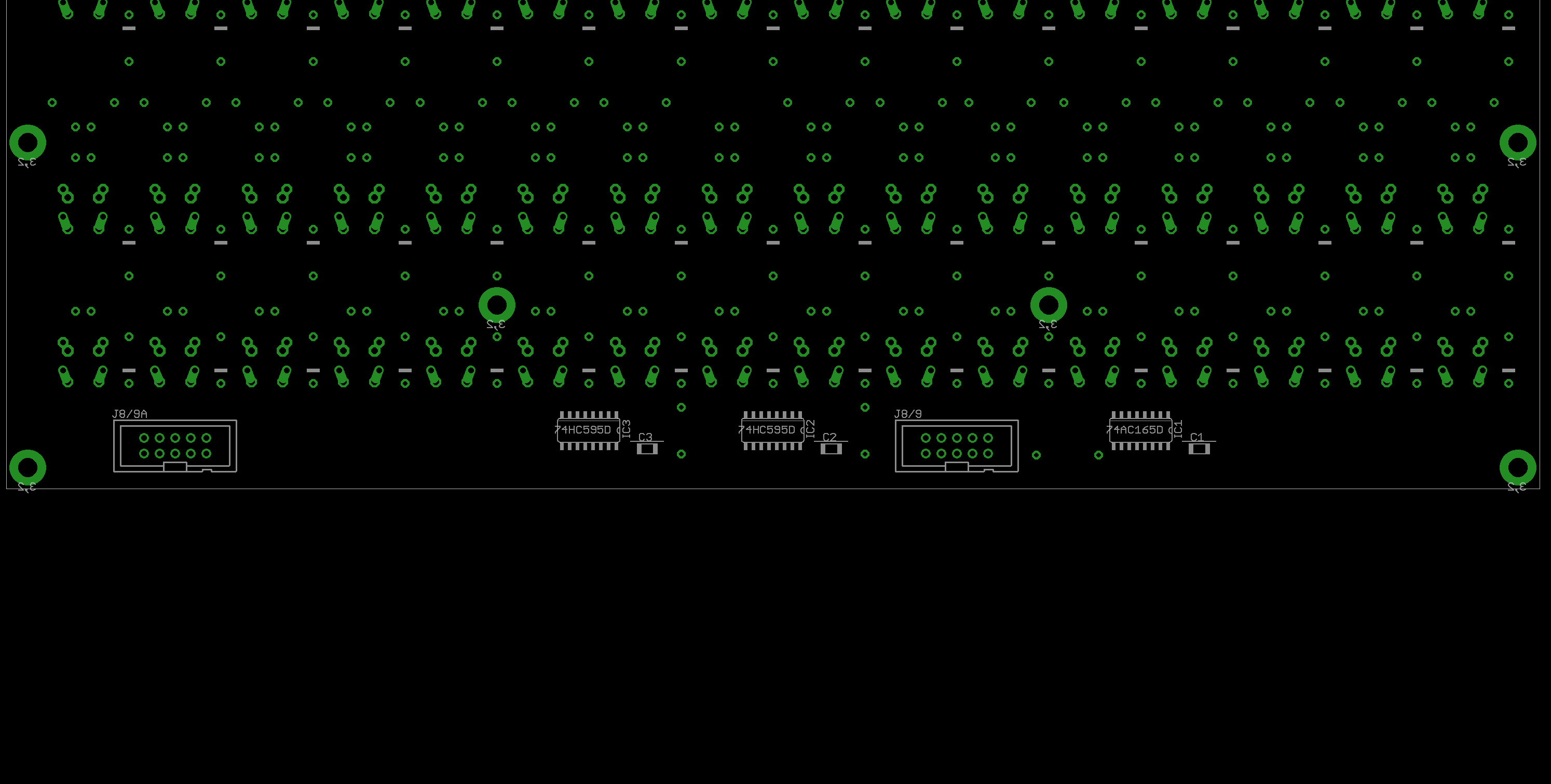
Rear placement of ICs (ignore the “AC” package, the correct CMOS family is 74HC165)
Assembly
Putting the board together is simple. As usual, start with the flattest components and work your way up.
SMT Components
- 3* 1206 capacitors
- 1* 74HC165
- 2* 74HC595
If you haven't soldered SMT before it's best to start here so you have a flat PCB to work with. A good strategy is to tin one of the (corner) pads with solder, then place the part with tweezers before forming a joint. Before continuing with others, ensure the part is correctly aligned by reflowing the single pad as needed. If it takes many tries, be sure not to overheat ICs. After a while the flux will be less effective at wetting the joint and so extra through a flux pen or similar is nice to have on hand.
It's good practice to visually and electrically check for short circuits between pads and remove excess solder with braid when required.
Resistors (+link), Diodes and Switches
- 9* 10k, left side (refer to PCB image)
- 8* 100R, right side (refer to PCB image)
- there's a set of dummy pads if you want the line of resistors to look symmetrical, it's just for show :)
- 1* LINK
- 48* 1N4148 diodes. Note carefully the alignment of the cathode band. The top two rows point “north”, while the bottom points “south.” If you get any of these wrong, the switches will not work.
- 64* LEDs, cathode marked by the flat part on the silkscreen. As noted, usually you will have 16 red and 48 green or other colour options. If you intend to build an opaque case, you may wish to install them “proud” i.e. only soldered once they're pushed up into the panel. For transparent cases, it's fine to mount them “flush” to the PCB.
- 48* switches. See part notes above. You can use different colours to help identify the different functions.
Headers
- J8/9 should be mounted on the rear of the board.
- J8/9A is optional for extending the SRIO chain (e.g. TPD, BLM etc.)
Interconnection to Core
J8/9 connects to J8/9 of a Core module (LPC17 or STM32F4).
Firmware
This file should be uploaded to an STM32F4 Core
The config file MBSEQ_HW.V4L should be copied to the root of the SD Card used. It can be found on the SVN repository.
At some point these should be made available in the normal MIOS32 download section.
A sessions folder will be created on first use if one doesn't exist. If you're having trouble with the MIDI Input, please open the SESSIONS/DEF_V4L/MBSEQ_C.V4 file and change:
MIDI_BUS_Options 0 0x00
to
MIDI_BUS_Options 0 0x01
License
Currently the design is © 2016 antilog devices with all rights reserved; all documentation is CC BY-NC-SA 3.0.