Table of Contents
MB-6582 (Prototype)
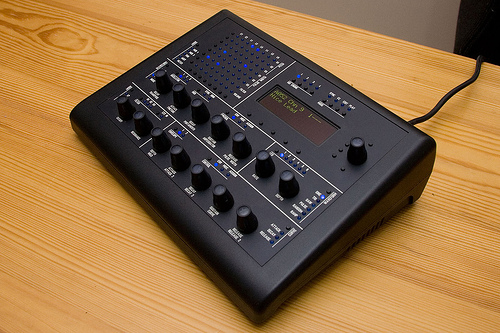
These are the wiki pages I wrote about the MB-6582, my MIDIbox SID Synthesizer V2 project. Since there were a lot of people who want the PCBs, and even to make their own identical box, I arranged a bulk order of the PCBs and other bulk orders of the panels and parts. Thus my original MB-6582 can be considered the prototype, as some changes (improvements!) were made for the PCB bulk order. As such, the rest of this wiki page is historical and has statements that I “will do” things rather than that I “did” them. Maybe I'll fix it up one day, but my time is better spent on the MB-6582 documentation
Introduction
MB-6582 is the name of my MIDIbox SID Synthesizer V2 project.
Ever since I started my first MIDIbox SID, I really wanted to put the whole thing on one single PCB, but stuck with the modular design of MIDIbox. I am glad I did it the modular way first, as I learned a lot about how it all fits together, and being modular is a lot easier to troubleshoot!
Modular vs Single PCB each has its own advantages and disadvantages… and so MB-6582 is more of a desire to implement a MIDIbox SID Synth idea, and follow through to completion, and not an argument for doing single PCBs or an argument against the MIDIbox modular spirit.
The idea, then, is multifaceted as well.
- I want a small case, not a 19“ rack case, or a refurbished C64 case (done that already!)
- I want to layout the PCBs (cos I love doing that!)
- I don't want lots of little PCBs to mount
- I don't want a mass of internal wiring
- I want it to look commercially-made and not obviously DIY, both externally and internally.
- I don't want screws visible on the front panel!
So this meant I had to find a prefabricated case (I'm not skilled enough or tooled up enough to make my own) and then design my own PCBs so I could pack as much into the small case as possible.
Finished Photos
You can view photos of the construction and other pictures here.
Construction Photos
You can view photos of the construction and other pictures here.
The Case
I didn't really hunt around for months for the best possible case, but when I came across the PT-10 case by PacTec, I was inspired. I loved how it had aluminium top and rear panels, was the size I wanted, and had enough room.
It was a good idea to start with the case and then make everything fit the case. The constraints of the case affects the front panel design and the PCB size and layout.
The Front and Rear Panels
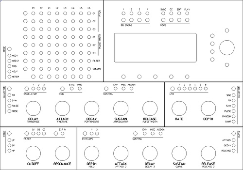
These will be white artwork on black anodized aluminium, made by Front Panel Express (a bit closer to me than Schaeffer, but essentially the same thing).
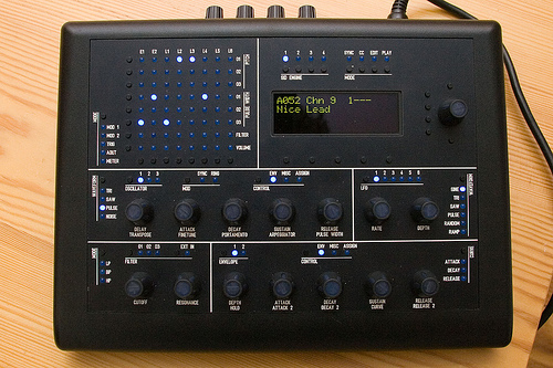
You can see this is a very minimalist design, and also very compact. In retrospect, the case constrained the layout of controls a little more than I originally thought it would, but its still quite functional and IMHO aesthetically pleasing.
I'll list the differences to the V1 “step C” control surface:
“Link” button replaced with “Sync”. This will be my global toggle between internal BPM and sync to external MIDI clock. I want to easily switch between playing a bassline in time with the external sequencer, or during development when I just want to play it without the external sequencer running. TK agrees this is a Good Idea so I might not have to code this feature myself Wink BTW, the “Link” feature is obsolete with proposed hardware changes, using PIC18F4685 and a CAN bus to the slaves.
“Play” button: this will replace the “SID button + Menu button” to trigger playing a note on the SIDs.
Extra buttons around menu encoder: The four to the right of the display I might use for fast selecting of a row on the display… maybe for the wavetable or sequencer pages. The buttons above and below the encoder are the “Menu” button and an undefined “extra” button for some feature I might want later.
Matrix mode select button and LEDs: Pretty self-explanatory, switches matrix into the other modes, V1 lets you switch between the mod matrix and metering mode, and I've expanded that to the proposed extra matrix modes. The names “Mod 1” and “Mod 2” are generic on purpose.
Filter Ext-In button: Since I plan to use the feedback idea (routing SID output through a pot into SID input), I wanted an easy way to toggle filtering of external in.
Missing “O3” LED in filter section: If I had the space space, I would put it in, with its own button.
“Misc” mode in Envelope section: A second set of parameters for envelopes, as described in the V2 wishlist.
“Curve” buttons/LEDs: Originally this was “Curve Assign” like the V1 feature (but missing from the “step C” panel) so I added it. Now it might not be needed if there's a separate curve parameter per envelope phase! So it might be used for another purpose… perhaps to multi-select envelope phases and let the Curve knob change those curve parameters.
“Ramp” LFO waveform: I always wanted a ramp. I'll code it myself if I have to!
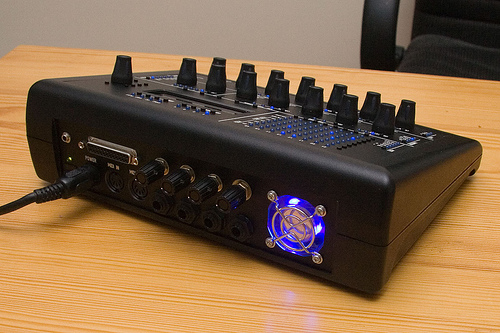
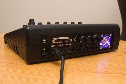
The rear panel has a few “extras” too:
Mixed output: Above the power switch/LED is a mixed audio output. If there are no plugs in the SID 1-4 audio jacks, the audio gets mixed through some 10K resistors. It's not that elegant a solution, but good enough for the times I just want to listen through headphones or plug it into someone else's amp or something.
Expansion port: In case I ever get around to using external filters or external analog inputs (joysticks, ribbon controller) or whatever else I can dream up, I can wire it through this 25 pin sub-D. I think I'll make it female like a printer port.
Four “feedback” knobs: The holes above the audio jacks will host four dual-gang 500K log pots, which attenuate the SID audio out on its way back into the SID. These can give effects like a resonance boost, self-oscillating filter, or distortion. They're log pots, so I still have to work out which way round they should go!
Fan hole: I'm sticking a 40mm fan in that hole. It's half-bling and half-functional… a little breeze inside that small box might just prevent SID death on a 40ºC summer day.
The PCBs
Laying out the PCBs was a slow process, because while it was fairly easy to layout each of the modules, I had to move them around a bit to make everything fit, and I continually changed my mind on what was going into it! I first thought I would leave the IIC_MIDI modules out and just mount some homemade ones as a temporary workaround to the PIC18F4620's EUSART bug. Then I decided I should put two in, since I liked the idea of a separate MIDI channel to the slaves.
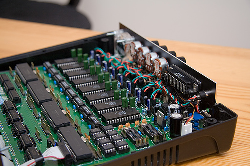
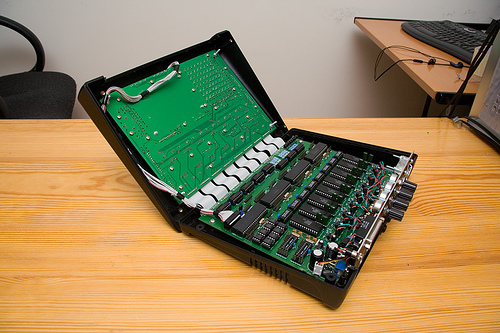
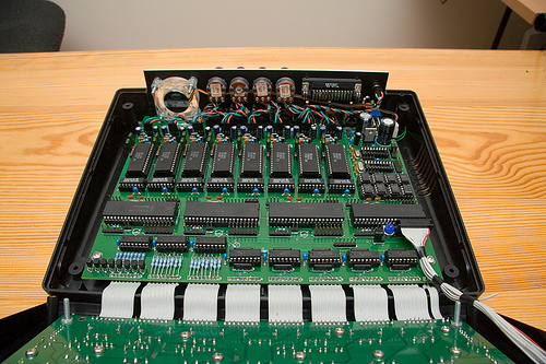
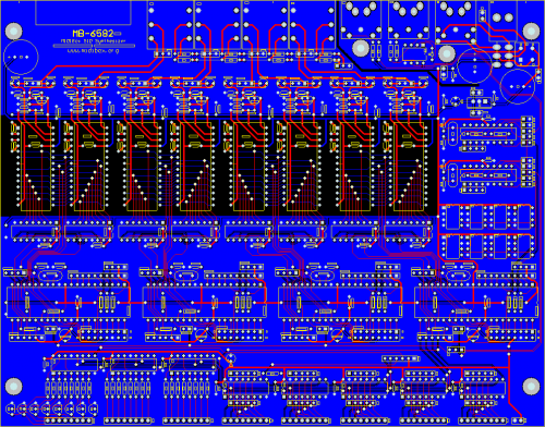
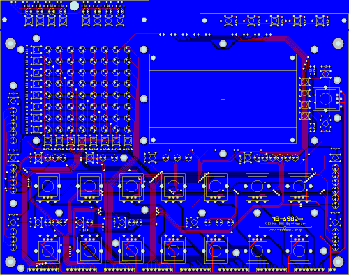
In the end, I've created two PCBs, one for the base of the case for the PICs and SIDs, and one that sits behind the front panel where the LEDs, switches and encoders are mounted.
The Base PCB
The base PCB contains:
- 4 Core modules
- 4 Stereo SID modules (8x SID chips)
- 8 “BankStick” chips
- 2 IIC_MIDI modules (Now redundant! Oh well!)
- 5 DIN modules
- 3 DOUT modules
- 4 stereo jacks
- 1 MIDI In, 1 MIDI Out, 1 optocoupler
- PSU section, regulating 9v AC to 9v DC (uses C64 PSU)
- C64 power socket and power switch
Four of the five DIN modules are used for the 15 encoders, the fifth is used to handle all the switches, which are in a scanning matrix. One of the three DOUT modules is both the current sink for the scanning matrix, and also the current sink for the LEDs in a 16×8 LED matrix.
Stereo SID module
Since MIDIbox SID Synthesizer V2 does not yet exist, a combination of intuition, educated guesswork, and emailing TK let me in on some of the details of the hardware for V2. The idea is that one Core can control two SID modules where the SID modules share all the current connections but have different “enable” lines. So each SID module's shift registers will have the same data clocked into them all the time, and then that data will be enabled into one SID, the other SID or both SIDs. This seems the most backward-compatible solution - no new hardware is required, people can choose to use one SID per Core for 4x mono channels, etc.
Since both SIDs in the stereo setup would have the same data presented to its address and data pins, you can connect just one pair of shift registers to both the SIDs.
I took the gamble that this intended design won't change, and got my PCBs built before V2 is even an alpha!
PSU
I will be using a C64 PSU, but the base PCB does not use the “C64 Optimized PSU” circuit. Since I don't use 6581s, I don't need a 12v supply to the SIDs, only 9v. So I didn't see the point of adding 9v DC to 5v DC to get 14v DC, only to regulate it back to 9v again! The PSU section of the base PCB just contains the required components to rectify and regulate the 9v AC to 9v DC, and joins this ground to the ground of the C64 PSU's 5V DC supply. I also use a single 9v supply to all eight SIDs, as it also seemed a bit pointless to use multiple voltage regulators. I use a single 9v supply to the four SIDs in my current MIDIbox SID and it seems to work fine.
The Control Surface PCB
The control surface PCB contains:
- redesigned “step C” control surface layout
- encoders, tact switches, 3mm LEDs
- mounts for the 4×20 PLED display
There's also two small PCBs with switches and LEDs mounted on them, which go above and below the display's bezel and are mounted via the display's mount holes. This allows the buttons/LEDs above and below the display to be closer to the bezel than would otherwise be possible if mounted on the control surface PCB.
The control surface PCB is designed to sit 10mm behind the front panel, which is just enough room for the PLED display to be mounted between the front panel and PCB.
The bottoms of the base PCB and control surface PCBs are joined together at the front edge of the case by eight ribbon cables of 0.1” (100 mils) spacing (i.e. standard SIL header or IC pin spacing). I've seen this kind of cable a few times when opening up consumer electronics. It made more sense to use 100 mils on the pads and cable so it's easy to solder and the cable can lie flat.
Rotary Encoders
The mounts for rotary encoders should work for either the 16mm ALPS encoders or the newer 12mm ones. I have the 16mm ones, they are clones of the ALPS STEC16B, probably the same ones I've seen from Voti.
Switches
The switches are ALPS 6mm TACT series switches. I may use 13mm ones, so they poke 1.5mm above the front panel, or fallback to using 17mm ones and shortening the shafts.
The swiches are connected into a scanning matrix. One 74HC595 (DOUT module) is used to sink the current of one group of 8 switches (through diodes). One 74HC165 (DIN module) is used to read the switch states.
LED Matrix
The LEDs I plan to use are tinted blue 3mm ultrabright LEDs.
All LEDs are connected into a LED matrix. One 74HC595 (the same one used for the switches) is used to sink the current of one group of 16 LEDs. Two 74HC595 are used to power one group of 16 LEDs at a time.
On the base PCB, there are 8 BC547 transistors connected to the 74HC595 used to sink the current for both switches and LEDs. This is a potential improvement to sinking the current directly by the 74HC595. Since all the switches have a diode between the switch and the output pin of a 74HC595, that's a 0.7v voltage drop, which is less than the 74HC165's maximum LOW level input voltage (1.35v at 4.5v supply). If I used a darlington array (ULN2803) to sink more current, then its voltage drop (collector-emitter saturation voltage) is about 1.1v at 100mA, so 1.1v + 0.7v > 1.35v. So I've used discrete BC547 transistors instead, which only have a 0.4v voltage drop when fully saturated (sinking 100mA of current).
Well, that's the theory. I did test sinking 16 of my LEDs through one fully saturated BC547 and the voltage at the collector really was 0.4v. I'm assuming there's enough time between the DOUT register update and the DIN registers being sampled for the BC547 to fully sink the current. If not, I'll just bridge across the transistors.
4x20 PLED display
I had a bit of trouble getting this display to work in 4-bit mode (the default for PIC18F4685, since two port B pins are used by the CAN bus Tx & Rx lines). Here's a custom LCD driver to use 8-b-t mode by using two pins from port E to replace the two pins on port B (i.e. D2 & D3). pic18f4685_8bit_lcd_driver

